We Help Contractors Thrive
With Our All-In-One
Sales & Marketing Platform
Get More Customers, By Making Sure YOUR Business Is Seen In Google Business Listings ABOVE Your Competitors
and NEVER miss another lead opportunity again

5/5 star reviews
See why we have such raving reviews
AS SEEN ON


Conversifi
Has everything Your Company
Needs To Succeed
1.Keep Ahead Of Your Competition and Get More Customer Enquiries
Being Ranked Higher than your competitors in Google Business Listings will get your customers to call you before them. We automate your Google Business review requests and ensure they are ALL 5-star rated

2. Automated Appointment & Estimate Reminders
How many times have you scheduled a phone call or sales meeting & wish either you or your clients received a reminder so that everyone shows up on time. We make that possible.

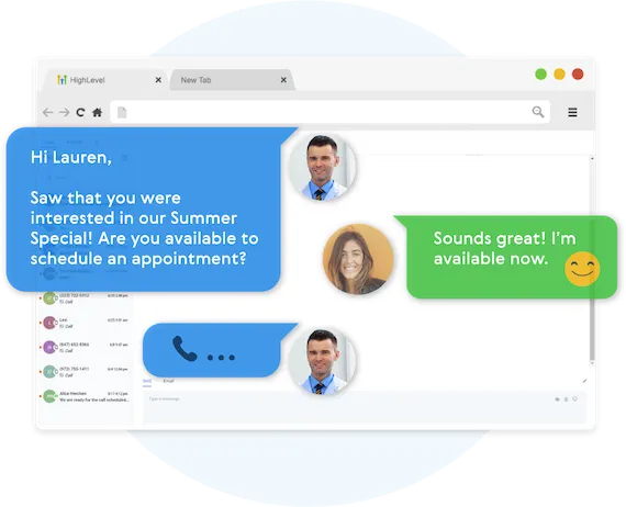
3.Speed To The Lead Is Essential.
Never miss a lead opportunity again if you are busy and can't take a call. Our automated Text Back feature will instantly send a text message to your customer if you can't pick up the phone, and will let you and them know that you'll get back to them very soon.

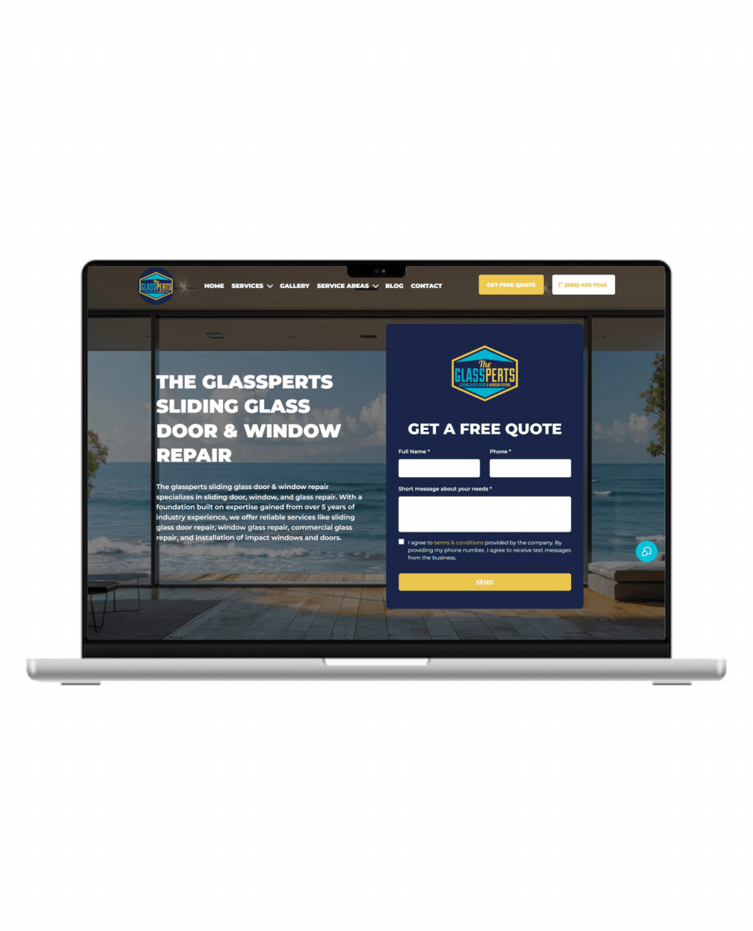
Fully Functional Website
Get a website that instantly turns leads into text conversations that go DIRECTLY to your phone.
Optimized For Local Google Searches
We make sure your Business has the best chance of ranking above your competitors in the Google Business Listings with full auditing and optimization.
Showcase Your Very Latest Reviews
Your latest Business Google Reviews will be automatically posted on your website for your customers to see.
Mobile Friendly
87% of people now visit websites on their phone. We will make sure your business looks the biz on mobile.
5-Star Magic Review Funnel
"Sure I'll leave you a review", but the truth is people forget. We’ll 'gently' remind them for a few weeks until they remember.
5-Star Review Only
You can’t make everyone happy, but our Magic Funnel makes sure you get Five stars, every single time.
Automatic Follow-Up Reminders
"Sure I'll leave you a review", but the truth is people forget. We’ll 'gently' reminder them a few times until they remember.
Ask For Reviews In One Click
Once a job is finished, simply click a button and your system will automatically kick-off the google review request on auto-pilot
Worried About Getting A Bad Review
Unsure if you should ask for a review in case its bad? Don't worry - we will guide your customer to leave a
5-star review only, or it won't get posted.
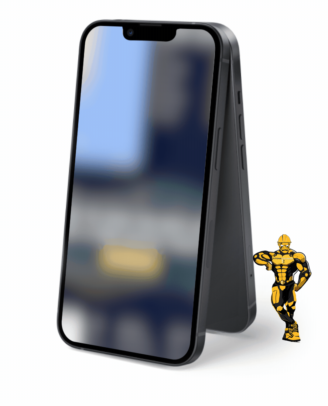
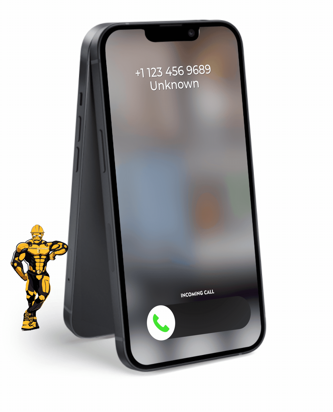
Missed Call Text Back
Everyone misses calls, but not everyone texts back. Be the one who does. Outshine your competition.
5-Star Review Only
You can’t make everyone happy, but our Magic Funnel makes sure you get Five stars, every single time.
Automatic Follow-Up Reminders
"Sure I'll leave you a review", but the truth is people forget. We’ll 'gently' reminder them a few times until they remember.
Ask For Reviews In One Click
Once a job is finished, simply click a button and your system will automatically kick-off the google review request on auto-pilot
Worried About Getting A Bad Review
Unsure if you should ask for a review in case its bad? Don't worry - we will guide your customer to leave a
5-star review only, or it won't get posted.
The Difference
Agencies Vs. Our Solution
Lengthy contracts: 3-4 months..
Zero trial period.
Expensive: £2,000+/month.
Lead generation solution.
Get You More "Leads"
No contracts.
14-day free trial.
Affordable: from £47/month.
Appointment generation solution.
Grow your online presence
Never Lose Another Lead Again
Automatically Nurture Existing Leads Into Customers.
Easily customize your follow-up Campaigns
Our Multi-channel follow up campaigns allow you to automate engaging follow ups and capture all responses from your leads, across all channels.
Create Multi-channel Campaigns
Conversifi allows you to connect with your leads through Phone, Voicemail Drops, SMS/MMS, Emails, GMB Messages, and even Facebook Messenger.
Two-Way Communication On Any Device
Our full featured mobile app allows you to communicate with your leads on all devices.
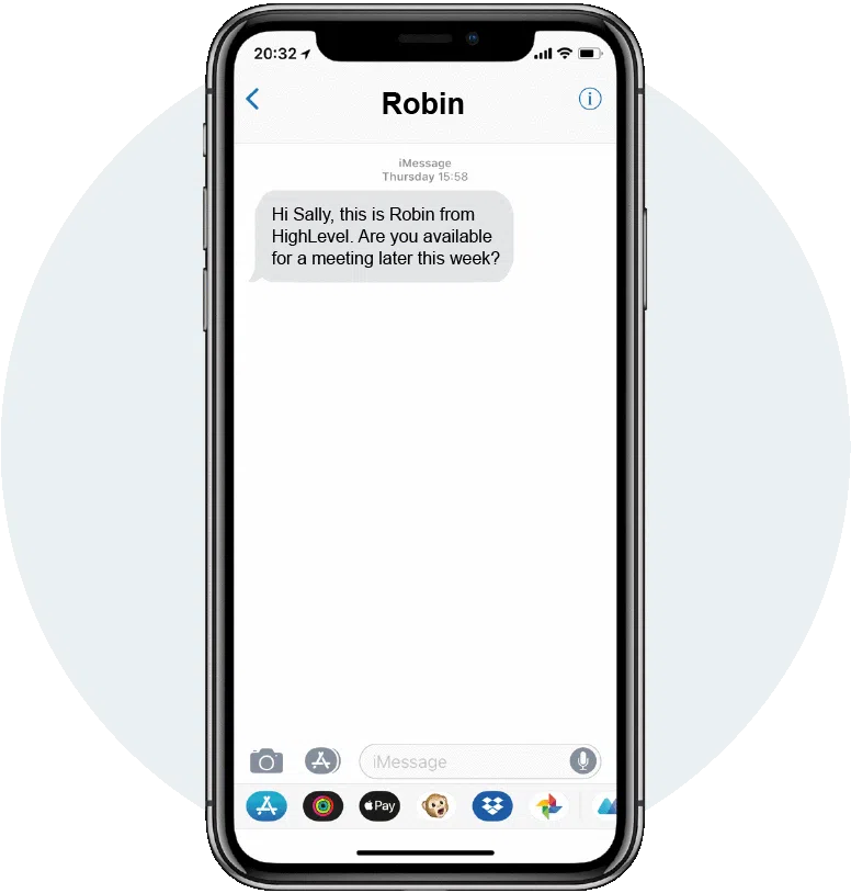
Fully Automated Booking
Automatically book leads and prospects on your calendar without lifting a finger.
Automated Nurture Communications
Create text conversations with the goal of placing booked appointments on calendars WITHOUT any human interaction if you so choose.
Full Customization Of Messaging
Use our campaign builder to customize the messaging.
Artificial Intelligence Built-In
Conversifi allows you to leverage AI (Artificial Intelligence) and Machine Learning to manage conversations
WHO IS THIS FOR
We Serve The Following Industries
Landscapers
Plumbing
Roofing
electricians
handyman
painters & Decorators
Windows & doors
tree surgeons
Kitchen makeovers
Bathroom makeovers
carpenters
fencing
flooring
cleaning services
lawn car service
home security
hvac services
furniture polishing and spraying
dog grooming
floor & carpet cleaning
STILL NOT SURE?
Satisfaction Guaranteed
We are committed to ensuring your complete satisfaction with our services. If, for any reason, you find yourself not fully satisfied with the results we deliver, please reach out to us. We are dedicated to resolving your concerns promptly and effectively, offering solutions such as additional support, service modifications, or other measures tailored to meet your specific needs. Our goal is to ensure that your experience with us not only meets but exceeds your expectations, reinforcing our commitment to excellence in serving your business needs.

To Book an Online Demonstration
Select an available date below on my calendar
On the chosen date I will send you a link where we can share my screen from your Desktop Computer or Mobile Phone where I will demonstrate how our software works
Copyrights 2023 | Conversifi™ | Terms & Conditions