Nanomanufacturing 2024, 4(2), 81-98; https://doi.org/10.3390/nanomanufacturing4020006 - 1 Apr 2024
Viewed by 1069
Abstract
►
Show Figures
Organic solar cells (OSCs) are becoming increasingly popular in the scientific community because of their many desirable properties. These features include solution processability, low weight, low cost, and the ability to process on a wide scale using roll-to-roll technology. Enhancing the efficiency of
[...] Read more.
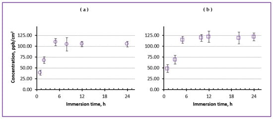
Organic solar cells (OSCs) are becoming increasingly popular in the scientific community because of their many desirable properties. These features include solution processability, low weight, low cost, and the ability to process on a wide scale using roll-to-roll technology. Enhancing the efficiency of photovoltaic systems, particularly high-performance OSCs, requires study into not only material design but also interface engineering. This study demonstrated that two different types of OSCs based on the PTB7-Th:IEICO-4F and PM6:Y6 active layers use a ZnO bilayer electron transport layer (ETL). The ZnO bilayer ETL comprises a ZnO nanoparticle (ZnO NP) and a ZnO layer created from a sol-gel. The effect of incorporating ZnO NPs into the electron transport layer (ETL) was studied; in particular, the effects on the electrical, optical, and morphological properties of the initial ZnO ETL were analyzed. The ability of ZnO films to carry charges is improved by the addition of ZnO nanoparticles (NPs), which increase their conductivity. The bilayer structure had better crystallinity and a smoother film surface than the single-layer sol-gel ZnO ETL. This led to a consistent and strong interfacial connection between the photoactive layer and the electron transport layer (ETL). Therefore, inverted organic solar cells (OSCs) with PTB7-Th:IEICO-4F and PM6:Y6 as photoactive layers exhibit improved power conversion efficiency and other photovoltaic properties when using the bilayer technique.
Full article

Figure 1

Figure 3

Figure 3 Cont.

Figure 4

Figure 5

Figure 6

Figure 7

Figure 8

Figure 9

Figure 10

Figure 10 Cont.


